The first thing to do is to read and understand Bill Wilson’s excellent gschem -> gsch2pcb -> PCB tutorial and/or the DJ Delorie’s pcb tutorial. This should get you started.
Also be sure to check out the other gEDA documentation available on this website.
However, the best way to learn the gEDA Suite is to download it and try it out yourself! If you consult Bill Wilson’s tutorial while trying the suite for yourself, you will become an expert in no time!
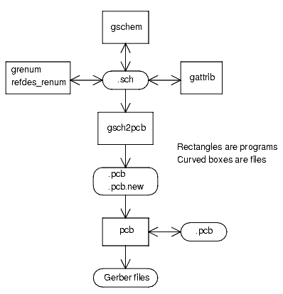
Here is a quick graphic for simple PCB design flow using the gEDA Suite:

In words, the design flow for a simple PCB proceeds as follows:
Create your schematic using “gschem”.
Check your schematics with the DRC checker. Learn about it
here.
Assign reference designators to your components using “grenum” or “refdes_renum” (or just attach them manually from within “gschem”).
Assign other component attributes (such as component footprints) using “gattrib” (or just attach them manually using “gschem”).
Create a preliminary layout file and netlist using “gsch2pcb”.
Lay out and route your board using “pcb”.
Output Gerbers from within “pcb” using “File → print layout”, and select “Gerber/RS274X” as the output file type.
If you make changes, or add to your schematic or attributes while in layout, update your board file like this:
Edit your schematic and/or attributes (”gschem” or “gattrib”).
Check your schematics with the DRC checker. Learn about it
here.
Forward annotate your changes using “gsch2pcb”.
From within “pcb”, update your components using “File → load layout data to paste buffer”, and then click on the drawing area to place the components.
From within “pcb”, update your netlist using “File → load netlist file”.
Usually, users invoke the individual tools from the command line. A project manager (”geda”) exists, but needs improvement.
The most important thing to keep in mind about gEDA’s limitations is this: GEDA is an open-source software project. It has some limitations, but unlike many instances of commercial software, its limitations are not artificial, arbitrary, or driven by marketeering. That is, gEDA is neither nagware, crippleware, demoware, nor “limited student edition”-ware. Any limitations to the gEDA tools exist because the programmers haven’t yet implemented that particular feature. Since the code is open for all to see and modify, anybody is welcome to implement a new feature or remove a limitation, and then submit their patches to the project. If you are a hacker and are interested in making a contribution to the gEDA project, consider tackling one of the limitations listed below! You will make a lot of friends, and earn international exposure!
Hierarchical bus support: Support for hierarchical buses doesn’t exist yet.
Net and pin attributes in gattrib: Attaching routing attributes for nets and pins in gattrib remains TBD. (Net attributes are useful for high-speed design. For example, it’s often important that all tracks in a bus have the same electrical length. Unfortunately, it’s not clear that PCB will support these routing attributes right now.)
Backannotation from PCB to gschem. Support for pinswapping and modification of the design file in pcb with subsequent backanno to gschem is TBD.
The project manager “geda” is out of date, and needs an update.
Layer count in PCB: Currently, the layer count in PCB is limited to 16 layers plus two silk layers by default. This is more than adequate for small- and mid-sized projects. If necessary, the number of layers can be increased arbitrarily at compile time.
A typical PCB design requires the following config files in your local directory:
gafrc: This holds configuration info for the gEDA/gaf programs (i.e. gschem, gattrib, gnetlist, etc.). It should hold pointers to your local symbol directory (if any).
attribs: If you use “gnetlist -g bom2” to create a project BOM, then you need this file in order to specify which attributes are written into the BOM.
projectrc: When going to layout, “gsch2pcb projectrc” is a convenient way to specify paths to local footprint directories, as well as hold other configuration information for “gsch2pcb”. Note that this file may have any name you choose; I like to use projectrc since its name is suggestive of its function.
Further detailed information about each configuration file is provided in the documentation for each facility.
The various gEDA/gaf applications (gschem, gattrib, gnetlist, etc.) use a set of RC files to set various configurable options in the tools themselves. These RC files are read in by each application upon start-up. Philosophically, there are three places where a gEDA/gaf application looks for RC files:
In the system installation directory: ${prefix}/share/gEDA/. This location holds RC files which are global to the entire system, and are common to all users. These RC files must be found and successfully loaded for the gEDA application to work properly. ${prefix} is set to the path where you installed gEDA/gaf.
In the user’s home directory: $HOME/.gEDA/. This location holds RC files which apply to all of this user’s projects. .gEDA is a directory. These files are optional. Do not just place a copy of the system-gschemrc (or whatever) into this directory; this will not work properly. The right thing to do is to override specific things you want to change.
In the local project directory. This location holds RC files which apply to the local project (which also lives in this directory). These RC files provide specific overrides, such as component or source libraries. This file is also optional. Do not just place a copy of the system-gschemrc (or whatever) into this directory; this will not work properly.
The RC file system has evolved over time. Originally, each gEDA/gaf application used its own RC file (for example, gschem used gschemrc, gnetlist used gnetlistrc, and so on). However, as the number of gEDA/gaf applications grew, it became clear that the individual RC files held a lot of redundant information, and that new users were confused by all the different RC files. Therefore, the different RC files were consolidated into a single file, called “gafrc”. However, because gschem needs all kind of special customizations, we decided to keep the system gschemrc in addition to all the gafrc files. Also, in order to preserve backwards compatibility, the old RC file system is still maintained in the system directory. Accordingly, the current RC file configuration looks like this:
In the system installation directory:
In the user’s ${HOME} directory:
In the local project directory:
Also loaded by the system-gschemrc is the gschem-darkbg or gschem-lightbg color definitions.
Finally, note that gEDA/gaf applications will look for up to six configuration files upon startup:
system-gafrc
system-gschemrc (or whatever)
${HOME}/.gEDA/gafrc
${HOME}/.gEDA/gschemrc (or whatever)
./gafrc
./gschemrc (or whatever)
If you get a warning that your app can’t find one or another of these files, don’t worry. Most of them are optional. The only required files are the system RC files.
The individual components in the gEDA design suite do not have the concept of an end-to-end project. Rather, they deal with their own files (e.g. “gschem” → .sch, “pcb” → .pcb). However, there is a project manager, called “geda”, which you can invoke from the command line. It’s goal is to help manage your design as a whole as you take it from concept, through schematic capture, attribute attachment, layout, BOM generation, and so on.
Unfortunately, development of “geda” has not kept up with the rest of gEDA/gaf. In particular, “geda” does not use the latest tools or methods to accomplish the individual design tasks. Therefore, we recommend that user simply invoke the individual tools (e.g. gschem, gattrib, gnetlist, gsch2pcb, etc) from the command line. Meanwhile, if your are a hacker are looking for a smallish project to adopt, polishing up “geda” would make a nice introduction to the gEDA Suite, and you would make a lot of friends by doing so!
We have a recurrent debate about XML file formats on geda-user every two or three years. I think it has to do with how long it takes us to lose our institutional memory due to churn on the mailing list.
It's unlikely the gEDA Project will ever switch to an XML file format for schematics or symbols, so get used to it. Some reasons against XML are:
GEDA/gaf already has a fixed, well documented,
ASCII file format. It's over 8 years old as of 2007. It's well used and well tested.
We already have a parser for our file format. It's lightweight & thoroughly debugged.
There are lots of legacy designs using the file format out there already. People would scream if we switched file formats since their old designs would become obsolete. And supporting two file formats – old and new – would be a major
PITA.
XML is a generalized file format. Therefore,
XML files tend to become bloated pigs. The gEDA file format is light & well adapted to its purpose: representing graphical information pertinent to schematic diagrams in electronics.
One purported benefit for
XML files is that there are lots of open-source parsers for them available, making integration into libgeda trivial. That's the theory, but in reality the job of a parser is to analyze and parse the input, and then stick it into datastructures suitable for use with the rest of gschem's code. An open-source parser does about 1/3 of the job we need (i.e. reading & analyzing the file, and creating some kind of parse tree). The rest of the job involves putting the stuff in the parse tree into libgeda's data structures. That's lots of work. Therefore, the purported advantage of the freely-available
XML parser is a chimera. Yes,
XML may be of interest for a new program written from the ground up, but not for an existing program like gEDA.
GEDA developer time is better used on implementing new features like backannotation. Using developer time on porting our file format to
XML is a sideways move which doesn't provide the end user any more utility, but soaks up valuable developer time.
The other benefit of
XML is that it is more-or-less human readable. I'll grant that this is a valid assertion. Our current file format is not readable by a human who has never read the documentation. However, our current file format *is*
ASCII, and is completely documented, so an essential reason for readability – the ability to write scripts against the file – is already taken care of. Also, a human can certainly read the file format once he has taken the time to
RTFM. Human readability – without knowing the file format – is a “nice to have” which isn't high on my priority list.
