This document describes the creation of component symbols, including style conventions, and hints/tips and things to look out for when drawing symbols for the gEDA/gaf system.
Component symbols (from here on known as “symbols”) are drawn using gschem. You can start with a blank page or a known-to-be good symbol that is similar to the one you want to create.
Before you open gschem to create your symbol, there are a few questions you should ask yourself, that will effect how you create your symbol:
Is this symbol purely for aesthetic purposes (a graphic)? If so, several steps are simplified.
Do I want to simulate the component in question, with e.g. Spice?
Do I want to use this symbol in a schematic that includes power distribution? This will become important when deciding what pins to draw.
Does this symbol represent a component that comes several in a package? This is called 'slotting' in gEDA's language, and has special rules.
Once you've answered those questions, the following guide will be more useful to you.
To start building your symbol:
Open gschem.
The default empty page has boxes on it. Use the selection tool (the one that looks like a black mouse cursor) to select everything on the page. Hit the Delete key to delete it.
Zoom in at least one step (View→Zoom, or hit the Z key).
Make sure the snap-to-grid functionality is ON (Options→Toggle Snap On/Off, or O S).
Make sure grid snap size is set to 100 (Options→Snap Grid Spacing…, or O Shift+S).
Use the 'line', 'box', 'circle', and 'arc' tools (in the Add menu) to create a simplified visual representation of your device. Make sure that the only colour you use is 'Graphic' (green). Do not place any pins on the device until the next step.
To check what colour you are using to draw, go to Edit→Color… (or hit E O).
If you have decided your symbol is graphical in nature (e.g., does not connect to anything, is just artwork), you can skip this step.
Add your first pin.
Select Add→Pin, or hit A P. Once that is done, click from the end of your pin, to one of the edges of your symbol. A '0' and the word 'unknown' should pop up near your new pin. Please note that the direction you draw your pins is important. If you draw them starting from the edge of your symbol to outside of your symbol, you will end up with text outside of the symbol!
Click on the selection tool, and use it to select the pin you just drew. The pin and text with it should change colors, and boxes should be drawn around the ends of the pin.
Select Edit→Edit…, or hit E E (or right click, and hit Edit…). This will bring up the edit dialog for this pin.
In the Edit dialog for a pin, you should see four attributes (name=value pairs) already associated with your new pin. These attributes can be edited by clicking on the attribute in the list at the top of the edit window, then clicking on the field you want to edit. Note that when selected, the Add Attribute section of this dialog does not reflect what has been selected, as it is only meant for addition, not for editing.
Let's look at each attribute already associated with your pin, and edit some of the values. I recommend expanding the size of the edit window until all attributes are visible.
All pins should have a pinseq attribute. This number dictates the order pins are looked at on this symbol in spice, gnetlist, and other tools. For our first pin, start this sequence number at '1', incrementing it on each new pin, as we add them.
All pins should have a pinnumber attribute. This is the number of the pin, on the package of the item you are drawing a symbol for. pinnumber values can be alphanumeric (i.e. like E or C).
All pins should have a pinlabel attribute. This attribute is the name or label of the pin (not the pin number).
All pins should have a pintype attribute. This attribute describes the kind of a pin.
pinseq and pinnumber attributes of several pins can be automatically numbered by Attributes→Autonumber Text….
Possible pintype values are: in, out, io, oc, oe, pas, tp, tri, clk, pwr. Please see the Master
Attribute Document for more info.
Every symbol needs some attributes (name=value pairs) in order to be useful in gschem, and in other tools.
First we're going to add all of the attributes we want, then make the ones that need to be invisible invisible.
A device=DEVICENAME attribute should be placed somewhere in the symbol. The devicename should consist of nothing but capital letters, dashes, numbers, and underscores. If the object is a graphic then device= should be set to none (device=none).
A graphical=1 attribute should exist somewhere in a symbol which is purely graphical (such as a title block or decon symbol). Symbols which have this attribute have no electrical or circuit significance. Don't forget to set device=none per the previous step.
A description=TEXT attribute should exist somewhere in the symbol. The TEXT value should provide a one line description of the symbol.
A
footprint=PACKAGENAME attribute should exist somewhere in the symbol which might be used with a pcb netlister.
PACKAGENAME is a pcb footprint or package type like DIP14 or DIP40. Please see the
footprint naming conventions page for further detail. If you are using gEDA / PCB, also see the
PCB documentation and gnetlist/docs/README.pcb for more info on this attribute and how it is used.
A refdes= attribute should be placed inside all non-graphical symbols. This attribute should default to U? for integrated circuits, and 'T?' for transistors. Make only the value visible and it will be promoted (attached to the outside of the symbol (so it can be edited)) when the symbol is placed in a schematic.
A numslots= attribute should be placed inside of all symbols, to prevent a warning when you will check your symbol by gsymcheck. numslots=1 works fine.
Now that those have been added, make the numslots, footprint, description, graphical and device attributes invisible. Leave only the value of the refdes attribute visible, and place it somewhere at the top of your symbol.
Add a label to your symbol by selecting Add→Text… or pressing A T. Type out your label, and move it to the top of your symbol.
Translate the symbol to the origin using Edit→Symbol Translate… or press E T.
Enter '0' into the entry field and press OK.
Save the symbol using File→Save or File→Save As…
Place the symbol in one of the directories specified by the component-library keyword in the system-gafrc file. Once this is done, the symbol should be visible immediately and can be selected and placed with the Add→Select Component… menu item. On Debian, placing files in /usr/share/gEDA/sym/local/ works, but require permissions setup.
Translating the symbol to the origin is a required step. To translate a symbol elsewhere, enter a offset (in mils) which is a even multiple of 100. Make sure all pins are snapped to a 100 mil grid point.
Symbols are named: symbolname-#.sym
Symbols end with a .sym extension.
Symbols have a -# where # is a number. Typically # is 1 but if there are multiple symbols for a device then this number simply increments.
Symbol names are typically lowercase but letters which are part of a part number are uppercase.
The above case rule can be broken if the filename looks incorrect or wrong.
This section describes the various requirements which must be met in order to create a valid symbol which will display and netlist in the gEDA/gaf system.
All pins should have a pinseq attribute. This number dictates the order pins are looked at on this symbol in spice, gnetlist, and other tools. This is just a sequence number, and should increment sequentially starting at 1.
All pins should have a pinnumber attribute attached to them. This is the number of the pin, on the package of the item you are drawing a symbol for. The pin number can be alphanumeric (i.e. like E or C).
All pins should have a pinlabel attribute attached to them. This attribute is the name or label of the pin (not the pin number). This attribute is also used when a symbol is used in a hierarchical schematic.
All pins should have
pintype attribute attached to them. This attribute describes the kind of a pin. Possible values are:
in,
out,
io,
oc,
oe,
pas,
tp,
tri,
clk,
pwr. Please see the
Master Attribute Document for more info.
For more information on the attributes presented here, please see the Master
Attribute Document.
A device=DEVICENAME attribute should be placed somewhere in the symbol and made invisible. Typically the devicename is in all caps (capital letters). This attribute should not be used as a label. Use a separate text object for the label. If the object is a graphic then device= should be set to none (device=none).
A graphical=1 attribute should exist somewhere in a symbol which is purely graphical (such as a title block or decon symbol). Symbols which have this attribute have no electrical or circuit significance. Don't forget to set device=none per the previous requirement.
A description=TEXT attribute should exist somewhere in the symbol. The TEXT value should provide a one line description of the symbol.
A
footprint=PACKAGENAME attribute should exist somewhere in the symbol which might be used with a pcb netlister.
PACKAGENAME is a pcb footprint or package type like DIP14 or DIP40. Please see the
footprint naming conventions page for further detail. If you are using gEDA / PCB, also see the
PCB documentation and gnetlist/docs/README.pcb for more info on this attribute and how it is used.
A refdes=U? attribute should be placed inside all non-graphical symbols. Make only the value visible and it will be promoted (attached to the outside of the symbol, so it can be edited) when the symbol is placed in a schematic.
The label= and name= attributes should not exist anywhere in the symbol. They are obsolete.
The netname= attribute should not be attached anywhere in the symbol. It is only used in schematics.
If a component has multiple slots in a package (such as a 7400 (NAND) which has 4 NANDs per package) then you need a numslots=# attribute. The # is the number of slots the device has. numslots= should be exist somewhere in the symbol and made invisible. Additional slot related required attributes are described below.
If a component has multiple slots in a physical package then you also need to include a
slotdef=#:#,#,#… for every slot. The first
# corresponds to the slot number. If a device has 4 slots then there should be
slotdef=1:…,
slotdef=2:…,
slotdef=3:…, and
slotdef=4:…, attributes existing somewhere in the symbol and made invisible. The subsequent
# have a one-to-one correspondence to
pinseq=# attributes and specify what corresponding
pinnumber=# should be when that slot is set. See the
attached 7400-1.sym as an example of how this should all work.
It is recommended that all symbols which have slots have a slot=1 attribute inside the symbol.
Running gsymcheck will check that all of these requirements are met. gsymcheck will output fatal errors which are quite serious and must be corrected. gsymcheck will also output warnings on things which should be fixed but are not fatal.
This section describes the style which is used in the standard gEDA/gaf symbol library.
All text labels should all be 10 pt in size.
Text (labels not attributes) should be color number 9 (text | green).
Use the special overbar encoding (e.g. pinlabel=\_Reset\_) to express inverse logic levels.
pinnumber attributes should be displayed as pin numbers for pins (not pinseq) and should be 8 pt in size.
Attached attributes should be color number 5 (attributes | yellow). The color is set automatically to yellow if the text item is attached.
The only exception to this is pinlabel= attributes, those should be color number 9 (text | green). If every text item within a symbol is yellow, the symbol looks too yellow.
Attributes can be attached to some part of the symbol. Toplevel attributes (like the device= or net= attributes) used to be required to be attached to something to be attributes, but now they just have to exist in the symbol file as name=value.
Expanding a bit on the last sentence, as long as the text item has the format name=value, it is considered an attribute. Attributes inside a symbol do not have to be attached to anything. In order to see hidden attributes in gschem select Edit→Show/Hide Inv Text.
There is a symbol content versioning system in libgeda which is based on the
symversion= attribute. Please see the
Master Attribute Document for more information on using this versioning scheme.
Lines, boxes, arcs, and any other graphics should be color number 3 (graphic | green).
Polarity bubbles should be color number 6 (logic bubble | cyan).
If you are unsure on how to make a new symbol look or how big to make a new symbol, look at the existing symbols to get a feel for the appropriate appearance and size.
Pins should all be 300 mils (3 grid spaces) long.
For pins which are next to a logic bubble, make the pins 200 mils (2 grid spaces) long and then make the logic bubble 100 mils in diameter. In order to draw a 100 mil diameter circle, you will need to change the snap spacing to 50.
A pin has two ends: one end has a red endpoint and one end that does not. The red endpoint is where nets can be connected. You can either rotate the pin so that this active end is in the right place or manually edit the symbol file changing the “whichend” parameter on the pin object. See the
File Format document for more info.
Be that all endpoints of pins which are meant to be connected to are on the 100 mil grid. The endpoint which is not active can be off the grid if necessary.
Pins should be color number 1 (pins | white).
Leave 400 mils (4 grid spaces) between (vertically) pins, unless you are drawing a special symbol, then just try to make it look good.
Pin number attributes should be 50 mils above (or below; which ever makes the most sense) the pin which they are attached to.
Input pins belong on the left and output pins belong on the right of the symbol.
Please do not mix inputs and outputs on the same side of the symbol, unless absolutely necessary.
You can have pins on the top or bottom of a symbol.
The order for rows of pins (buses) should be LSB (least significant bit) to MSB (most significant bit). When drawing pins which are part of a bus, make sure the LSB of the bus is at the top (or for pins on top/bottom of a symbol, left of the rest of the other pins). Look at 74/74181-1.sym for a correct example of this order (A0 on top through A3 and B0 on top through B3). Violating this rule will make connecting buses much more difficult.
When placing pins on logic gates, be sure to place the smallest pin numbers toward the top (or left) and then increment going down (or across).
-
The above rule can be broken if necessary, but keep in mind most of the standard library does not have power pins showing.
Keep in mind, symbols are supposed to be symbolic, they do not represent the physical package that the device comes in.
There is some disagreement on above, so this is okay too: arrange the pins on a symbol logically so that they promote an uncluttered schematic. Note that this is frequently not the same pin arrangement as the physical device.
This section describes some hints and tips which will make your symbol creation
experience easier.
Pins MUST be snapped on the 100-spaced grid.
Avoid drawing things off of the grid. If you do, you cannot move the object(s) using the move command (if the grid is on) since the object will be snapped to the grid. [This was an old bug, which I think has been fixed, but avoid doing this anyway]. Use the symbol translate command instead (or move the object with grid snap off).
It is okay to set the grid finer than 100 (say 10 or 25) when creating symbols, just remember to set this back to 100 once you are ready to translate the symbol to the origin.
If you want to translate a symbol from the origin to elsewhere, then use the Edit→Symbol Translate… command and enter a non zero number. Make sure this number is a multiple of 100 (i.e. 1000, or 1100).
Remember that pins are special objects; if you want to add a pin, make sure it is a pin and not a line or net. Use the Add→Pin command to place a pin.
Don't include nets or buses inside symbols. That is not supported and doesn't make much sense anyway.
pinnumber should be the visible attribute for pins, along with pinlabel if any.
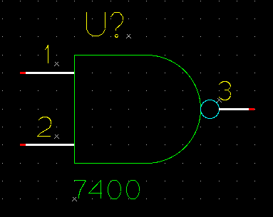
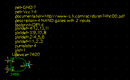
This section provides a simple example which tries to follow all of the above rules. This symbol is of a 7400 (NAND gate).
- 7400-1.sym
v 20031231 1
L 300 200 300 800 3 0 0 0 -1 -1
T 300 0 9 8 1 0 0 0 1
7400
L 300 800 700 800 3 0 0 0 -1 -1
T 500 900 5 10 0 0 0 0 1
device=7400
T 500 1100 5 10 0 0 0 0 1
slot=1
T 500 1300 5 10 0 0 0 0 1
numslots=4
T 500 1500 5 10 0 0 0 0 1
slotdef=1:1,2,3
T 500 1700 5 10 0 0 0 0 1
slotdef=2:4,5,6
T 500 1900 5 10 0 0 0 0 1
slotdef=3:9,10,8
T 500 2100 5 10 0 0 0 0 1
slotdef=4:12,13,11
L 300 200 700 200 3 0 0 0 -1 -1
A 700 500 300 270 180 3 0 0 0 -1 -1
V 1050 500 50 6 0 0 0 -1 -1 0 -1 -1 -1 -1 -1
P 1100 500 1300 500 1 0 1
{
T 1100 550 5 8 1 1 0 0 1
pinnumber=3
T 1100 450 5 8 0 1 0 2 1
pinseq=3
T 950 500 9 8 0 1 0 6 1
pinlabel=Y
T 950 500 5 8 0 1 0 8 1
pintype=out
}
P 300 300 0 300 1 0 1
{
T 200 350 5 8 1 1 0 6 1
pinnumber=2
T 200 250 5 8 0 1 0 8 1
pinseq=2
T 350 300 9 8 0 1 0 0 1
pinlabel=B
T 350 300 5 8 0 1 0 2 1
pintype=in
}
P 300 700 0 700 1 0 1
{
T 200 750 5 8 1 1 0 6 1
pinnumber=1
T 200 650 5 8 0 1 0 8 1
pinseq=1
T 350 700 9 8 0 1 0 0 1
pinlabel=A
T 350 700 5 8 0 1 0 2 1
pintype=in
}
T 300 900 8 10 1 1 0 0 1
refdes=U?
T 500 2250 5 10 0 0 0 0 1
footprint=DIP14
T 500 2450 5 10 0 0 0 0 1
description=4 NAND gates with 2 inputs
T 500 2850 5 10 0 0 0 0 1
net=Vcc:14
T 500 3050 5 10 0 0 0 0 1
net=GND:7
T 500 2650 5 10 0 0 0 0 1
documentation=http://www-s.ti.com/sc/ds/sn74hc00.pdf
This example produces the following (using gschem):

This is the same symbol with all the hidden text visible (via Edit→Show/Hide Inv Text):


